
 12 hours ago
3
12 hours ago
3

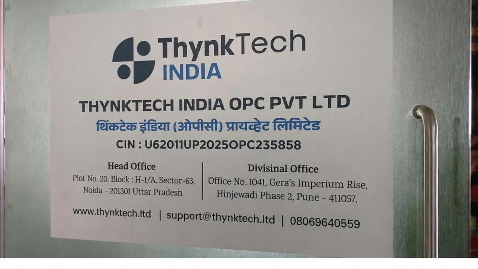
The Andhra Pradesh government has finalised the arrangements for its first semiconductor project under the India Semiconductor Mission (ISM). The groundbreaking ceremony for the Outsourced Semiconductor Assembly and Test (OSAT) facility, proposed by M/s. Advanced System In Package Technologies Private Limited, is scheduled for June 8.
The project, proposed at Tarluvada village of Anandapuram mandal in Visakhapatnam district, envisages a total investment of ₹2,387.81 crore. The investment will be executed in two phases. The first phase will involve an outlay of ₹542.19 crore, followed by ₹1,845.61 crore in the second phase.
“To ensure the rapid grounding of this high-tech facility, the State government has approved the allotment of 30 acres of land to the firm at a nominal rate of ₹1 per acre. This is a special case and a maiden project sanctioned to the State under the Union government’s India Semiconductor Mission,” a higher official told The Hindu on Wednesday (June 3, 2026)
The project is expected to be a major employment generator for the region, with plans to create 1,000 jobs—200 in the first phase and 800 in the subsequent phase.
![]()
The government has extended special incentives under the Andhra Pradesh Semiconductor and Display Fab Policy (4.0) 2024-29. These incentives are capped at 40% of the project cost and will be released on a ‘pari-passu’ basis, aligned with the disbursement of the 50% grant provided by the Union government.
Infrastructure push
The State government has directed the Andhra Pradesh Industrial Infrastructure Corporation (APIIC) to oversee the development of essential external infrastructure, including roads, power, and water supply, with costs to be borne by the IT, Electronics and Communications (IT, E&C) Department.
The revenue, energy, and municipal administration & urban development departments have been instructed to work in tandem to ensure the seamless execution of the project.
As per reports, this development marks a pivotal advancement for the local technology sector, positioning the district as a key node in the country’s semiconductor manufacturing ecosystem.


 English (US) ·
  French (CA) ·
  French (FR) ·